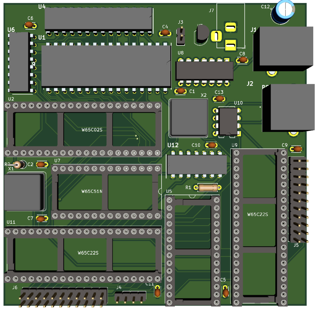
With my second build, I’d successfully tested the hardware, memory and I/O devices I wanted to use in my third build, my planned handheld unit. Eager to move on, I quickly drew up a schematic and laid out a PCB for my planned design. Consistent with a handheld unit, I wanted to keep the PCB small, say 100 mm square. At this size I’d also qualify for discount pricing at some PCB manufacturers.
I went through many iterations of the PCB layout before settling on a design I was happy with. I created both a 2-layer and 4-layer version to give me some flexibility in choosing a PCB manufacturer. I expected routing the 2-layer board would be more complex than the 4-layer board but this wasn’t the case. More on that in another post.

The computer has the following features:
- WD65C02 microprocessor running @ 1 MHz (though higher speeds are possible)
- 32k byte SRAM
- 16k byte NOR flash (banked memory possible with added jumpers)
- Jumper for 480×800 LCD display (interfaced with a WD65C51)
- Two WD65C22 VIA with breakout jumpers for expansion
- PS/2 keyboard connector (interfaced with ATtiny85 and one of the VIAs’ shift register)
- USB connector for serial communication (through second WD65C51) and power
- Alternate barrel jack for power
- Power-on Reset
- Jumper for reset switch/button
With the PCB design in hand, I was ready to look into having it manufactured. Or was I? Could I be certain this design would work? True, I had tested all of the components, either on my second build testbed or separately. But I hadn’t tested it all together according to the schematic above. I felt pretty confident in my design, but stories of other’s problems with their first PCB were nagging. Would I have a similar experience? How could I be sure I was ready to move forward?
As a first check, I reviewed the designs and PCB layouts of several 6502 builds I found online. It wasn’t long before I discovered that I had placed the PS/2 keyboard connector backwards. What other problems lurked? How would I find them? Another breadboard build seemed a logical route. A breadboard build would also give me a testing platform for this design should I have problems with the PCB.
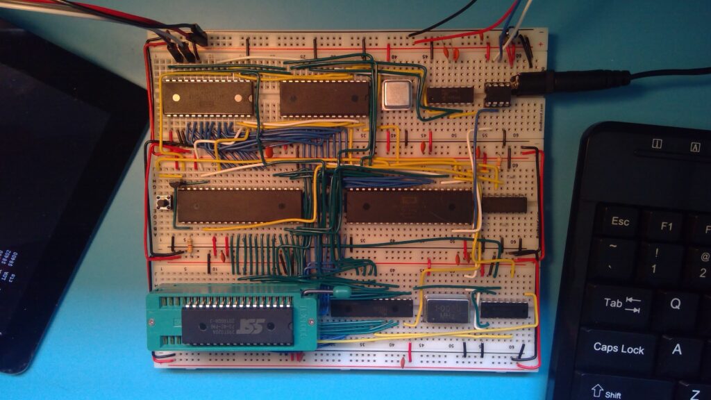
I quickly built a third 6502 breadboard computer. With a bit of preplanning, I made it as compact as I could, keeping in the spirit of my goal for a handheld unit. I arranged the chips to shorten the address and data pin wiring and created a small data bus running down the middle of the board. I left out one of the 65C22s due to space considerations and reused the crystal oscillators and ZIF socket from my second build as I didn’t have spares for those on hand.

Troubleshooting
Being my third breadboard build, I felt pretty confident prior to powering up my latest creation. After a few tweaks to my monitor program to reflect the new memory map in this build, I powered it up to a blank display. My monitor program should have output the results of some self-tests it runs on start up, but I got nothing. At first, I suspected that I hadn’t connected the display correctly, but I soon found out that the 65C51 wasn’t transmitting any data at all. I then suspected I made an error is assigning/wiring the correct I/O chip select signal to the display, but a quick check showed everything appeared ok with that.
Finding nothing apparently wrong with the display portion of the circuit pointed to a more serious issue. A review of my wiring against the schematic showed no apparent discrepancies so I needed to dig deeper. Luckily, I have a logic analyzer. The compactness of my build made it a bit more difficult to attach than with my second build, but I had left open connections on the breadboard to accommodate this.
Hooking up my logic analyzer to the address and data busses quickly identified a problem, the 6502 wasn’t reading the proper reset vector during its startup sequence and the 6502 was continually reading from the interrupt vector location. After verifying that the 6502 wasn’t receiving an interrupt signal, the behavior pointed to a problem with the address and/or data busses. Turns out I had problems with both.
Due to the compactness of my build, I had tested the continuity of the address and data busses early in the wiring stage. I was pretty confident that I had everything connected properly. Obviously, I didn’t. On the address bus I inadvertently connected address line A15 from the 6502 to the ROM chip in both the schematic and build. This meant that I was reading from a higher address range on the chip than where my monitor program was actually written. Worse I had left the ROM chip address line A16 floating in both the schematic and build. Strangely I had tied address line A17 to ground in the build as I had done that in the second build but I had not reflected this on the schematic where I had left it floating.
Fixing the ROM chip address wiring gave a more normal sequence on the address and data busses on startup but the monitor program still wasn’t starting properly or outputting anything to the display. Examining several erroneous bytes of data revealed I had likely transposed two data lines. This seems strange since I had validated that wiring early in my build. Then I remembered that I had disconnected a portion of the data bus to ground an input signal on one of my 65C51 chips. Checking that wiring, I found that I had indeed reconnected two of the lines in reverse.
After fixing the data bus I was confident again powering up my build. Surely it would work now. No such luck. The display remained blank and no output was apparent on the 65C51 transmit pin. My logic analyzer showed however, that my monitor program was running normally. Zooming into the region of the program where the 6502 was accessing the 65C51 chip I found that the I/O chip select signal wasn’t going low when the 6502 was trying to access the chip. That pointed to a problem with the address decoder portion of the build. After a bit of troubleshooting, I found I had reversed the A and B inputs to the ROM and I/O portion of the 74HC139 chip. I’d done this on both the schematic and build. I then remembered that on an early layout of the PCB I had reversed the inputs to create a more efficient routing, not realizing that this altered the I/O chip select signal (the ROM chip enable signal wasn’t affected). After fixing this everything worked as expected.
Lessons Learned
I was a bit humbled working through this third breadboard build. I started so confident after making my schematic and PCB layout only to find out I had problems with both. Similarly, I was confident my breadboard build would work right off the bat, but, even if my schematic was error free, I had made errors in the wiring, even though I had carefully checked my work as I went along.
At this point I think my third build schematic and PCB layout are more solid but I’ll leave confidence in it until after I have a board manufactured and assembled. I’ll likely start off with a 2-layer version of the PCB that I can get made inexpensively so I can test the design. A 4-layer version will be more expensive. I might make one just for testing and comparison even if the 2-layer version works fine. But I’ll leave all of that for another post.
Have you had similar confidence in a design only to find it didn’t work when you finally built it? Tell me about it in the comments.
A great read! I’ve never attempted a PCB build, although it’s definitely on a far flung agenda. Would you be interested in creating a series of posts explaining all the elements of creatiing a PCB? The majority of PCB posts definitely don’t start from scratch, and I’m guessing that there would be a decent audience for a set of blog posts that dealt with each major step.
Anyway, thanks for your blog – it’s a fascinating subject and you write well. More please 😁
Thanks for the blog post idea. So many things to do and so little time. My next post will likely be about my new Forth based operating system for my 6502. Forth is a fairly obscure language nowadays, but has some appeal in memory constrained systems and where the user wants direct access to the underlying hardware. I’ve been working on my own version over the summer, just for fun. It seems a thing. I’ve seen jokes online saying there are more people developing Forth systems than are actually using Forth systems. I suppose I’m helping continue that impression.
PCB design was challenging but was quite doable even starting out as a beginner. The key is just taking it step by step. I used Kicad (kicad.org) for the PCB discussed in this post but as you can imagine, that’s the result of many hours trying out all of the steps on smaller, sample projects. It’s best to get started working through a couple of the Kicad tutorials to get up and running.
Also there are several different PCB design alternatives so be sure to check them out as well. Kicad has some quirks that I believe are handled with more polish is other design packages.
I’ll be attempting to build a Forth system too. 🙂 Actually it’s my main motivation for building a 6502 comp. I’m hoping I might actually write something in Forth at the end of it….
I’ve actually got Forth running on my third build now. It’s been pretty fun and has mostly kept me from my build and blog. I just got block read access on an SD card for loading words coded in Forth during start up Write access should be straight forward. I’ll get around to writing about it some time as it’s got most of the features I need.
The last week or two a few of us have gotten a game from 1982 written in Forth working on modern systems. I got it working on my Forth. You can read about it here.
Mark, I can recommend John’s Basement’s videos: https://youtube.com/playlist?list=PL3by7evD3F51fKkyrUbH-PCdwPCWc9F8a
I’ve found them to be really helpful.