My first 6502 build, which followed Ben Eater’s 6502 computer project, has a 16 character by 2 line LCD and a single red LED for output and four push button switches for input. Ben stopped his original video series with just a single push button, but I added three more as pictured on the front of his 6502 kit.
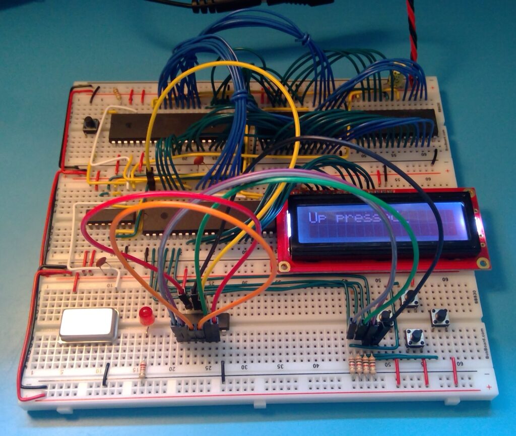
Though fairly basic I/O considering the potential capabilities of even this simple computer, it was sufficient to explore the 65C02 processor and 65C22 versatile interface adapter (VIA) further.
Shown above, I’ve interfaced the 4-button input to Port A and CA1 on the VIA. The VIA is set to latch Port A on a CA1 positive edge thus capturing the button pressed through the corresponding bit on Port A. With the CA1 interrupt enabled, the VIA then requests an interrupt from the 65C02 which then reads Port A and prints a message to the LCD, indicating the button pressed.
I imagine this is something like what Ben planned to do when he developed his kit. I guess he left that for us to explore as more recently he’s moved in a different direction, augmenting his 6502 series with videos on VGA and PS/2 keyboard interfaces.
My Second 6502
I left my first build intact awaiting future videos from Ben and started another. I intended my second 6502 build as a testbed to try out ideas for an envisioned third (and final?) 6502 build, a handheld unit, say something like the MOnSter 6502 handheld interface (as seen in the MOnSter 6502 project video).
Or perhaps something similar to the original Acorn Microcomputer.
As a testbed, my second build, shown below, has had many components, mainly I/O related, added, tested, and perhaps even removed if something better came along.

The massive address/data/control bus on the right is used to facilitate interfacing with many different I/O devices. In hindsight, it was overkill. If I do something like that again, I’ll probably just incorporate it into a small section on the main build and daisy-chain the connections between devices.
VIA vs PIA? Oh my!
You might be able to see that the 16×2 character LCD display in my testbed is interfaced with a 65C21 peripheral interface adapter (PIA) rather than a VIA as in build one. The PIA is similar to its VIA cousin but lacks the timers and shift register and thus, as the naming implies, isn’t as versatile.
I was thinking of a build with a PIA/VIA pair, having the PIA handle the LCD display leaving the VIA fully free for other devices. The PIA is a dollar cheaper than the VIA and has an extra chip select pin that would perhaps add flexibility in using wasted I/O address space.
After a quick glance at the PIA datasheet, I thought that the LCD related code for the PIA would be almost the same as that for the VIA. That wasn’t the case. The 65C21 has only 2 register select pins versus 4 on the 65C22. This complicates interfacing with the chip and changing modes, such as reading from a port versus writing to it. It takes more instructions to do this on the PIA than on the VIA. To me, the easier programming and faster execution alone justifies the added cost of the 65C22 and I would add two VIAs instead of a PIA/VIA pair, even if I wasn’t planning on utilizing the extra timers and shift register.
And Along Came ACIA
I added a 65C51 asynchronous communications interface adapter (ACIA) and USB to serial breakout board soon after starting my second 6502 build. I was working on a monitor program and had tired of the process of reprogramming the EEPROM after each iteration. I wanted to be able to load a program directly to RAM for testing. Additionally, the serial interface would provide the keyboard input needed to do anything meaningful with my monitor program, at least until I added a dedicated alphanumeric input device.
Soon after getting this serial load-to-RAM interface working, I installed a ZIF socket for my EEPROM and found I could reprogram it from power down to power up in less than 10 seconds. This was far faster than the process to properly format and load code to RAM through the serial interface. As such I haven’t used that capability since. In fact, I removed the USB to serial breakout board. It’s related 65C51 interface chip is now used to interface the 4D Systems display, shown to the right in the picture above. That display replaced a larger character LCD module (40×4). More on those decisions later. I retained the 16×2 LCD for debugging purposes only, the character LCD functions having been almost totally replaced by the 4D Systems display. A character LCD will not make it into my handheld unit.
Getting the ACIA working was more challenging than the VIA, likely because it involved interfacing with the USB-serial board as well as properly setting up a PC serial terminal. Midway through the process I bought a digital analyzer to help troubleshooting. You can just see a glimpse of it in the top center of my second build picture above. The ribbon cable and most of the jumpers in the photo feed it signals from my build. It proved invaluable as a source of high-resolution debugging info. I don’t think I would have solved the issues without it. I’ll discuss using my digital analyzer further in a post on tools.
Note that the WDC65C51 has a bug (now considered by WDC to be a feature difference from earlier designs). Interrupts cannot be used to control data transmission. Rather a delay must be used to ensure that the transmitter shift register is empty before it is reloaded. A long thread at 6502.org discusses the issue and gives possible alternatives.
One alternative is to use the original 6551 if you absolutely need interrupt driven serial transmission. I have successfully tested the chip as a drop in replacement for the 65C51 in my second build (meaning it worked successfully with my existing code which doesn’t use interrupt driven serial transmission). If you want to go this route then make sure to check out the discussion thread above as it mentions some other issues with older chip as well.
Many hobbyists have opted to use other UARTs in place of the ACIA. Some seem driven more by the desire not to use a “defective” chip in their system. However, the work to incorporate a non-65xx UART seems to be more than incorporating the transmission delay required by the 65C51. I may move away from the ACIA at some point, but for now it works in my system so I’ll stick with it.
On a side note, the Sparkfun serial breakout board linked above has an annoying “feature” of putting stray voltage into my build through its data and control lines even though these were only connected to my ACIA. This didn’t seem to affect the 6502 operations but did cause some puzzling multimeter readings during troubleshooting. I didn’t look into this further after I removed the board. More recently I discovered the Microchip MCP2221A that performs the same function in a more convenient DIP-14 package. This chip will definitely make it into my third build.
And Then There Was Tiny
Coincidently, about the same time Ben posted his PS/2 keyboard hardware interface video I was at the point of adding my own keyboard interface. Ben’s interface design, while educational, wasn’t really suited for my handheld goal. It added three ICs, used a full port on the VIA and relied on the 6502 to process the PS/2 keyboard scan codes. I wasn’t willing to give so much up for so seemingly a basic task – hit a key, get an ascii byte representing it.
In researching the interface issue, I discovered that a controller chip, now long out of production, was used in old computers to interface with the PS/2 keyboard. To replace this capability, some hobbyists take an approach like Ben and build an interface from basic logic circuits. Others emulate the old control chip with a modern microcontroller.
I used to think it a bit silly to use a device many times more powerful than the 6502 as an interface chip in a hobby build. After all, why not just build a system around the microcontroller and do away with the 6502 altogether? For me the answer became clear as I worked through my monitor program, examining old Apple II code for ideas. The 6502 for me has a nostalgia that the modern microcontrollers will never have. I fondly remember working with the same code long ago. For me, working with the 6502 is fun. A modern microcontroller doesn’t inspire the same feeling. It’s powerful and capably, but it’s just a tool used to accomplish a task.
And so, I’ve used an ATtiny85 to interface the PS/2 keyboard to my 6502. The chip is indeed tiny, an 8-pin DIP, ideal for my handheld unit. I use two pins for the PS/2 keyboard clock and data lines to capture scan codes. I programmed the ATtiny85 to translate these to an ascii byte and use two other pins to send the byte to the VIA’s shift register. While the ATtiny85 is just a tool to accomplish this task, I must admit that it was fun to work with it.
I actually crossed this retro vs modern bridge earlier when I chucked the 40×4 character LCD module in favor of the 4D Systems display. Actually, that experience probably led me to consider using the ATtiny to interface the PS/2 keyboard. The 4D Systems display is in many ways, more powerful and functional than the 6502 system I’m building behind it. It has a faster and more capable processor, more memory, and more I/O interface capability. But I use it just as a tool to accomplish the task of displaying data, much like the ATtiny85 is a tool for processing input from the PS/2 keyboard.
Both of these are powerful additions and I may use them to further expand the capabilities of my handheld 6502 system. File storage is one example. I haven’t thought much about it yet other than buying a few chips to test out on my testbed. But why not just use the 4D System display extra flash memory and/or SD card slot. I don’t see much difference in using the 4D Systems storage or the Microchip SST39F020A flash memory chip I bought for testing. For me the storage is just another tool to facilitate the use of my 6502 system.
The added power doesn’t eliminate all issues though. The 4D Systems display itself is rather slow. The 6502 can spit out data many times faster than the 4D Systems display can display it on screen. The bottleneck appears to be writing to the display itself as the serial interface and display microcontroller seem to handle buffering the data stream just fine. This really isn’t an issue for it’s anticipated use, but does mean that I won’t be using this display for gaming.
I suppose this too could be solved with more powerful hardware, but at this point gaming is not it’s intended use so I guess I’ll cross that bridge when I come to it. Besides, the 4D Systems display is by far the most expensive component in my planned handheld unit. I can’t imagine spending more for something more capable. At some point you get back to the question of whether it’s really a 6502 system at all. I’m not going to draw a line beyond which I won’t cross right now. I’ll leave the purity of build philosophy to those concerned with such things.
Measure Twice, Cut Once
I also learned in my second build that I need to take more care in planning the layout of my I/O devices, even on a testbed meant to be somewhat fluid. Originally, I had the board with the USB to serial interface at the bottom of the build which wasn’t a great location for connecting a USB cable. I later move the board to the top of the build making room for the keypad interface which was more naturally placed at the bottom of the build. It was then that I learned that the breadboards don’t like to be physically moved after you’ve stuck them to the surface below with their adhesive foam backing. I lost a good portion of the foam backing on the USB board when making that move. Now that I know that, I’d just redo the circuit onto a new board instead. Live and learn!
Changing Visions
You’ve likely realized from the above discussion that my envisioned handheld unit has morphed as I’ve progressed with testing I/O devices. Starting with a decidedly retro look, with matching functionality, I found my planned keypad and 4-line LCD I/O very limiting. For example, the disassembly of a portion of my monitor program on the 4D Systems display, as shown in my second build picture above, demonstrates the inadequacy of limiting output to just four lines. Yes, I could work with a 4-line display, but why when I could do so much more with something else.
Also, the 40×4 character LCD is ridiculously large compared to the amount of data it can display. It is several inches wider and only an inch less in height that the 4D Systems display that can easily display 15 times the amount of data. I liked the retro look of 40×4 LCD, but didn’t want to sacrifice that much functionality or have to expand the size of my handheld unit for it. I hadn’t even fully programmed its interface before I chucked it in favor of the more capable display.
The keypad proved a bit more versatile, as I expanded its capability by programming the ‘0’ key to also act as a shift key. This allowed the upper three rows of keys to serve as control keys in addition to their normal use. With 12 control keys and the original 16 hexadecimal digits, I was able to accommodate all of my monitor program functions, but only just. The setup was still pretty limiting. To go further with just the keypad for input, I’d have to add a second or third shift key, assigning even more functionality to the keys in the upper three rows. I didn’t go that route though. You can just see a hint of the PS/2 keyboard in the early stages of testing in the upper right corner of my second build picture.
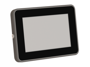
My current vision for my handheld unit is a more modern, tablet type of system, similar to that pictured below, with an external PS/2 keyboard.
I still like the idea of separate keypad unit for the retro vibe but my interface for it takes up large portions of one VIA and two logic ICs, which would consume valuable PCB space. As such I doubt it will make it into the final handheld design, at least not without modification. Maybe a job for another ATtiny? Or maybe I can move some of the interface ICs onto a separate PCB housed in the keypad enclosure. I’ll leave that for a future project.
It is possible to have the 6502 perform all of these interface functions, but then it would have less time to do other things (see this PS/2 keyboard interface for example). It might be fun to see how far I could push the 6502 but as I’d get little use from the resulting code, I’ll leave it to some time when I have nothing more interesting to do. This exposes one of my evolving design philosophies. Unlike some 6502 hobbyists who eschew technology not available in the early 1980’s, I’m willing to use modern tech to interface with peripherals.
How about you? Do you use a mix of modern and old tech in your 6502 designs? Or are you more of a purist, keeping your designs as true to the vintage as possible? Tell me about it in the comments.