The 6502 microprocessor can address a 64k byte range. As a system designer you must split this address space between RAM, ROM and I/O according to your requirements. My first 6502 build, which followed Ben Eater’s 6502 computer project, used a straight forward memory map with 16k bytes of RAM (address range $0000-$3FFF), 32k bytes ROM ($8000-$FFFF), and I/O addressable in the remaining range ($4000-$7FFF). Thus, when the 6502 addresses $0500 it is accessing RAM. Similarly, at address $F000 it is accessing ROM and at address $4100, I/O.
An address decoding circuit is used by a 6502 system to “select” whether RAM, ROM or an I/O device is enabled when the processor is addressing a particular address, as specified by the system’s memory map. Several design requirements must be meet when setting the memory map for your system. These requirements tend to constrain the possible address space split between RAM, ROM and I/O. The availability of appropriately sized RAM and ROM chips might further drive your memory map decisions. Other design decisions may also affect your memory map and may even result in what some consider “wasted” address space. As with other things 6502, the web has a wealth of resources on 6502 memory map and address decoding options. Garth Wilson’s 6502 Primer has a page on both here and here. Ben Eater has a good video discussion on address decoding here.
For my second 6502 build I tried an alternative address decoder discussed on Ben’s subreddit that gives 32k bytes of RAM (address range $0000-$7FFF) and 24k bytes ROM ($A000-$FFFF) with I/O addressable in the remaining range ($4000-$7FFF).
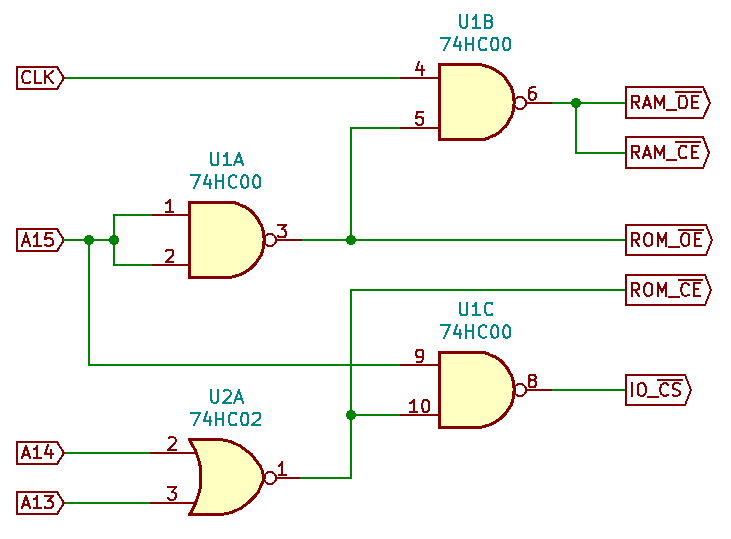
This gives the memory map below showing regions where RAM, ROM and I/O devices are accessible. For example, I/O device #1 is addressable at $8010-$801F. If the 6502 address bit A4 (pin 13) is tied to the device’s active high chip select pin and the I/O active low chip select signal on the address decoder (pin 8 on the NAND chip) is tied to the device’s active low chip select pin, the device will be enabled when the 6502 accesses memory in this range. RAM, ROM and other I/O devices as needed, are connected to the 6502 address bus and address decoder circuit in a similar way according to the memory map and address decoder logic.

This memory map accommodates up to nine I/O devices, each with 16 addressable registers to interface with the device. This provides a large enough address range to accommodate the family of 65C02 based peripherals. Address bit A4 and above can be used as register select bits as well if you need to access a larger group of registers on some other I/O device. In that case you’ll lose access to one input device for every additional address bit used. If you had to access up to 256 bytes on an AVR device, for example, you would have to use address bits 0-7 for I/O register select, leaving address bits 8-12 available for chip select on five I/O devices.
I’ve highlighted several regions in gray, which I’ve labeled as non-addressable memory. Accessing memory in one of these regions will enable more than one I/O device (other than $8000-$800F in which no I/O device is enabled). Trying to do so may result in conflicts on the data bus for reads or writing to more than one I/O device with perhaps unintended consequences.
An address decoder can be designed according to your system requirements for RAM, ROM and I/O devices. More complex decoders can optimize the split of the address space and sometime capture some of the non-addressable space created by simpler circuits. However, there may be a tradeoff. A system with a more complex address decoder may not be able to run at as high a clock speed due to propagation delay in the decoder. Propagation delay is the time for the address decoder outputs (chip enabling signals) to respond to its inputs (various 6502 address bits or the clock).
Here is a trace showing the propagation delay through the NAND/NOR address decoder above at 1 MHz. We can see the chip select signal (magenta trace) is only slightly delayed compared to the input signal considering the overall clock cycle length of 1000 nanoseconds.
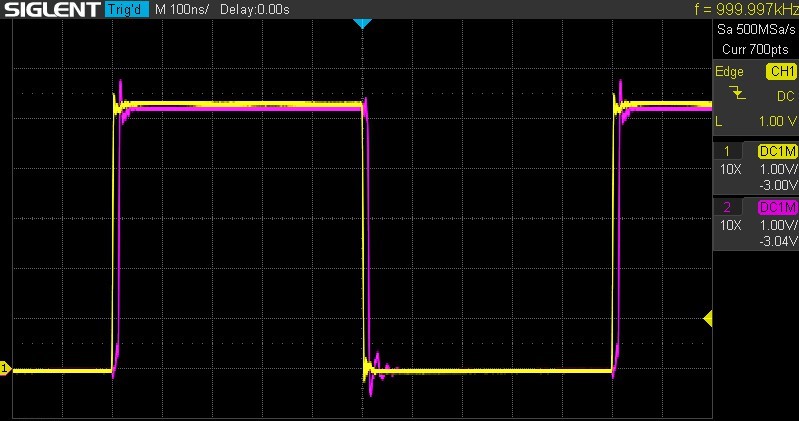
Zooming in we see that the propagation delay is about 12 nanoseconds or a bit over 1% of the clock cycle length.

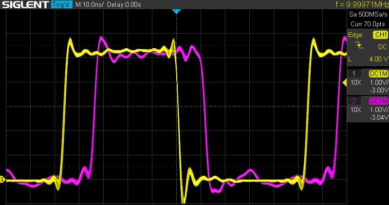
I’ll take a closer look at address decoder propagation delay in a future post, but below is the trace of the same address decoder circuit above at 10 MHz. Notably, the propagation delay stays the same while the clock cycle length is now only 100 nanoseconds. Getting the chip enable signals though the address decoder now consumes about 12% of the clock cycle. You can imagine that your address decoder can’t get a lot more complex if you plan to operate your system at high clock speeds.
For my third 6502 build, a handheld version, PCB board space will be at a premium which puts the two chip address decoder used in my second build at a disadvantage. With that in mind I searched for one chip solutions (as I used in my first build) but with a larger portion of the address space devoted to RAM rather than ROM.
One option discussed here, gave a memory map with 32k bytes of RAM (address range $0000-$7FFF) and 16k bytes ROM ($C000-$FFFF) with I/O addressable in the remaining range ($8000-$BFFF), basically the reverse of that of my first build. This loses 8k bytes of ROM compared to my second build, but since I’m currently only using a bit over 4k of the ROM, I’m going to go with this address decoder for now. The decoder uses a single 74AC139.

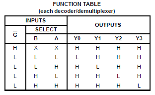
The 74AC139 is a dual 2-line to 4-line decoder. It has a function table as follows.
The resulting memory map is as follows.
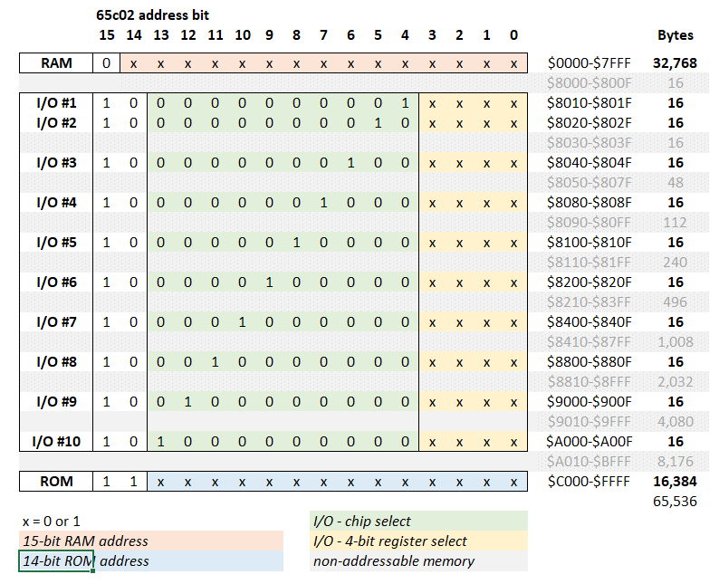
Compared to my second build I’ve gain another possible I/O device but lost 8k bytes of ROM, most of that going to non-addressable space. Not a totally satisfying solution. The 74xx139 was the only off-the-shelf decoder I found, but the link above mentions a few other custom single chip decoders, that I might try out in future builds, though I’d have to have a compelling reason to do a build four.
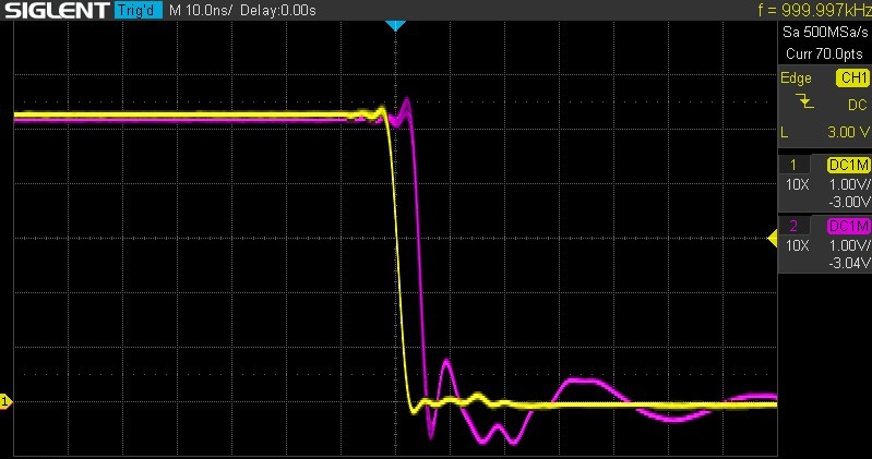
All that remains is to look at the propagation delay through the 74AC139. At about 4 nanoseconds, it’s significantly better than the NAND/NOR decoder used in my second build.
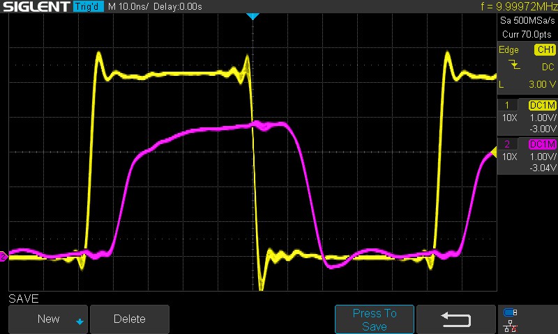
You might be familiar with the 74LS version of the decoder chip from Ben Eater’s 8-bit computer output module video. You should think twice about substituting that chip for the 74AC version as it has a propagation delay of about 18 nanoseconds. Here is a trace of it with a 10 MHz clock. You can also see from the trace that the output doesn’t respond as cleanly or reach 5 volts as the 74AC version of the chip.
Do you have a favorite memory map or address decoder for the 6502. Tell me about it in the comments.
By the way, some images are missing? 74AC139 Address Decoder, for example?
Hmm… Thanks for pointing that out. Everything is showing up just fine for me. I’ll look into it more from some other device.
Update: everything shows up for me on my phone, in a different browser and in incognito mode which seems to remove the possibility of stuff showing up just because I created the content. The 74AC129 memory decoder circuit diagram can be found here. Other images are available as well by editing that link and browsing the uploads directory.