I had just finished building and testing my fourth 6502 build, a barebones testbed for my new PLD based address decoder. With my PLD successfully tested, the build didn’t really have much use anymore, except testing new PLD designs in the future. Given that it was barebones I figured it would be fun to see what it would take to get it running with a 65C816, WDC’s 16-bit version of the 65C02.
The 65C816 is not a drop-in replacement for the 65C02, but most of the pins are the same and of the five that are different, most don’t need to be considered for simple designs like the ones I’m building. A quick look at the data sheets shows only two pins of these five need to be changed between the two chips. The rest are not connected.
| Pin | 6502 | 65816 | 6502 Use | 65816 Use |
| 3 | PHI1O | ABORT | NC | tied high |
| 7 | SYNC | VPA | NC | NC |
| 35 | NC | E | NC | NC |
| 38 | SOB | MX | tied high | NC |
| 39 | PHI2O | VDA | NC | NC |
| 9-20,22-25 | A0-A11, A12-A15 | same | ||
| 26-33 | D7-D0 | same | ||
| 8,21 | VDD, VSS | same | ||
| 1,2,4,5,6 | VPB,RDY,IRQB,MLB,NMIB | same | ||
| 34,36,37,40 | RWB,BE,PHI2,RESB | same |
Essentially, to get a 65C816 to work with a basic 65C02 build, the pin 38 connection to 5 volts needs moved to pin 3. Note that some folks might not tie pin 38 high on their 6502 builds, but it appears you have to tie pin 3 high on the 65816. I couldn’t get mine to run properly without it.
No other changes are needed. Note that for my fourth build, discussed in my last two posts, I had to remove the capacitor on the write enable signal. But since that addition shouldn’t have been necessary, I don’t consider it a needed modification.
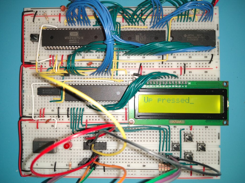
With build 4 running with a 65816, I wondered if my other builds would be as simple. The answer is yes. Here is my slightly enhanced Ben Eater 6502 build running with a 65C816.
And here is my build 3 running my Forth operating system on a 65C816.
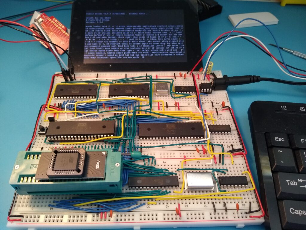
Of course, I can’t access additional banks of memory with this build (even though it’s there on the board). But I can test out the other 16-bit features of the 65C816. I plan to do just that with my third build. Perhaps I’ll ultimately upgrade my fourth build to more fully accommodate the 65816 and banked memory. But for now, I’ll stick with my build 3 running a 65816 given it is more capable. I’ll probably start with a modification of my Forth operating system to take advantage of some of the 65816 features.
PS – 7/4/2022
Forum member sburrow over on 6502.org posted W65C816 pinout compared to W65C02 with the twist of including the 65C02 as a drop-in replacement for the 65816. He mentions that the bank address and data bus buffer circuit “will work generally” with the 65C02. It’s not exactly clear what he means here. In 65816: Modifying Build 4 as a 65816 Testbed I mention I had to remove the bank address latch chip to get the build running with a 65C02.
Sburrow recommends replacing the ‘573 with a ‘273 with “/E (not emulation) on /MR will automatically switch to Bank 0 whenever in emulation mode, thus simulating the 65C02”. When I was starting my 65816 build, I considered the ‘273 as a ‘573 replacement because it was the only similar chip I had on hand at the time. I don’t think I fully understood that the flip-flop would “latch” the bank byte until the next high clock transition. Generally, it looks like the ‘273 will work. However, when LE is high on the ‘573 it’s passing through the data input pins to the output. The output data on the ‘273 won’t change until the next clock transition, delaying the memory set up. I suppose this could mean that a faster memory is needed in a ‘273 system than would otherwise work in one with a ‘573.