I worked on the Build 4 modifications over several weeks, partly because I was just playing around with what I had on hand when I started and partly getting sidetracked looking into why things happen instead of just getting on with the build. In this post, I discuss modifying Build 4 in more detail. In another post I discuss a side investigation into the PLD that’s featured in this build and in another post, I discuss troubleshooting the memory corruption issues I found.
Having gotten my barebones 6502 build 4 to successfully startup with a 65816, I decided to use it as a testbed of sorts to continue tinkering with the 65816. I’d need to add keyboard support. No problem. I’d left room in the middle of the build for that. I also wanted to enable switching the build to the 65C02 to test out new PLD designs for that processor as well. I’d have to consider that when making modifications.
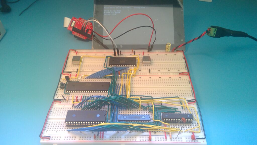
The data bus running down the middle of the board would make adding keyboard support easy, similar to that on Build 3. In fact, I’d have to borrow the ATTiny85 from that build for a bit because the chips are out of stock, I suppose due to the chip shortage. Stupidly I had skipped buying some from Jameco.com recently when they had them on clearance and the next time I looked, they were sold out. Ultimately, I bought a small development board that included the chip. It cost a few bucks more, but I wanted both builds to be fully operational for easy testing and comparison, especially since Build 3 was able to run with a 65816. This proved useful in the troubleshooting I faced ahead.
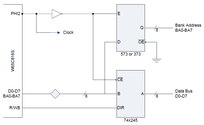
Another natural addition to Build 4 for 65816 tinkering would be WDC’s suggested bank address latch and data bus buffer circuit.
I decided to use 74HC versions of the logic chips. With those I’d be ready to compare and contrast with the W65C816SXB Development Board. What fun! Many skip right to 74AC chips here as the HC versions don’t seem to quite cut it, especially in breadboard build. I picked up the AC versions as well, just in case. I was rewarded for this foresight, as we’ll see later.
I decided to start simple, adding just the data bus buffer. It would fit perfectly right above the processor and wouldn’t require much rewiring. Just install the chip backwards, move the processor’s data pin wiring to the 245 B pins and connect the A pins back to the data bus. I’d also need an inverted clock signal for it, but luckily I had one free output pin on my PLD so adding it was as simple as reprogramming it and wiring it to the 245. Oh, the joys of PLDs.
You’d think that this simple modification wouldn’t affect the operation of my build. After all, I just added a data bus buffer that simply passed the data back and forth between the processor and the data bus at the proper times. Basically, nothing that would seem to affect normal operations. But firing up the build after this addition led to disappointment. I’d get the startup splash line and then an error indicating the Forth code of my operating system wasn’t loading properly. After a lot of testing, I found I could get the build to run with a 55 ns RAM chip. Interesting, since the build ran fine with a 65C02 with 12 ns RAM. And the W65C816SXB Development Board runs with 10 ns RAM. More on troubleshooting that in my next post.
Having at least temporarily gotten my build to start up with the slower RAM, I decided to add the keyboard support and bank address latch circuit as well. The only open space on my board for the bank address latch was the upper right which would require running wires to the processor data pins on the other side of the board. Looking at my build, it made more sense to the position bank address latch directly above the processor and the data bus buffer above the data bus in the center of the board. That would leave just enough room for the 65C51 and crystal oscillator on the upper board to the right. It would require a bit of rewiring, but two-thirds of my build could stay intact.
I decided to to ahead and rearrange the upper board to more naturally accommodate the bank address latch and data bus buffer. While I was at it, I decided to add support for the upper memory ROM in the chip I was already using. That would give me a chance to actually test banked memory. It would be more natural to add extended RAM, but I didn’t have the required chip and that would also require a more extensive rewiring.
I’ll probably have another post on it, but I’ll just mention here that it required an entirely different memory map as the PLD couldn’t accommodate simply adding the expanded ROM to the address space I’d been using. Luckily, I found an address map that would give me access to the extended ROM I had on board without adding another chip, which I didn’t have room for.
This all required me to do a fair amount of rewiring. Similar to before, I used off-the-board wiring to allow the chips to be more easily extracted for testing. I knew from experience that this wasn’t good for speed, but since that wasn’t a purpose for this build, I wasn’t concerned. Well, that would come back to bite me. More on that in my troubleshooting post.
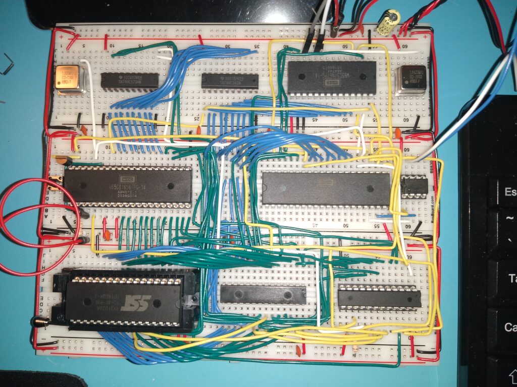
I decided to add a ZIF socket for the ROM as well. I found that the Aries model combined with a 28-pin IC socket worked well with my breadboard. Without the IC socket it didn’t stay as firmly seated on the breadboard as I would like. I got ZIF socket from Jameco.com, but their website has been offline for some time now so I can’t provide a link.
Firing this bad boy up leads to? Nothing. Drat. More troubleshooting. That shouldn’t be hard, right? After all, rewiring aside, the only difference compared to the earlier version was the addition of the bank address latch.
Here’s where breadboards and my layout paid off. I popped out the 573, grounded A16 and A17, used to access extended ROM, and fired it up. Success. So, the problem is with the bank address latch.
The natural next troubleshooting step would be to test with the 74AC573. Luckily I had some on hand. Popping one in proved successful. But why. The W65C816SXB Development Board worked just fine with a HC version of the chip. And the HC245 in the data bus buffer seemed to be sufficient as well.
As you’ll see in my next troubleshooting post, I’m driven more by investigating why things happen than simply making them work. So, my project will be sidetracked some more while I track this down. I already have a clue. Jobi_wan on Reddit, posted about how he fixed his 65816 build. He had been generating his inverted clock signal with an inverter, but switching to a 74×74 flip-flop to generate a synchronized clock and inverted clock, solved the problem he was having. With foresight, I included an HC version of the chip in my last chip order.
In Troubleshooting 2 I’ll see if that solved the problem with the 75HC573. It shouldn’t be necessary. WDC uses an inverter HC573 for the bank address latch, but perhaps that doesn’t cut in on a breadboard build. Stay tuned.
PS
By the way, Build 4 continued to run with a 65C02 and 12 ns RAM throughout all of my troubleshooting by simply removing the 573 and grounding A16 and A17. During troubleshooting the 65816 with 55 ns RAM however, I concluded that the PLD was likely causing memory corruption problems, perhaps similar to those wvenable discussed in his Reddit post. To confirm that, I removed the PLD and connected a traditional address decoder circuit in its place. With the 65C02, everything worked as expected.
With the PLD back in place now, the 65C02 version of the build continues to run fine with just the bank address latch removed. Given what I learned in Troubleshooting 1 I’m beginning to think the PLD is fine and that the issues I’m seeing are due to the tolerances of the particular 65C816 chips I have being tighter than those of my 65C02. More on that in Troubleshooting 1.
PPS
Occasionally, for added assurance, if needed, it was a simple matter to remove the 245 and jumper the A and B sides to connect the data bus to the processor.