I completed my fourth 6502 build the other day. It’s a barebones build, mainly intended to test my new PLD-based address decoding/interrupt request design. I didn’t need serial or keyboard support to test the PLD so haven’t included quite a bit of the I/O support that I had in build 3. I’m thinking that I’ll base my ultimate handheld on a 65816 so this 4th build probably won’t be used for much beyond PLD testing.
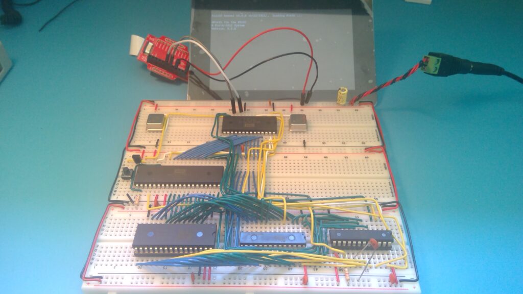
I debated just modifying my third build but decided to start fresh as it’s nice to have a reference build when things don’t work as expected. I’ve seen that with my previous builds, and such was the case with this build too, as we’ll see.
I used a breadboard layout very similar to my third build but used slightly arched paths for the data and address bus wiring between the memory chips. This results in slightly longer wires but much easier breadboarding. That gave me a few issues on my third build. I’m not planning on doing much speed testing with this build, so keeping the data and address bus connections as short as possible wasn’t really an issue.
I was hoping for things to work right away but based on my third build wasn’t too optimistic. Sure enough, I didn’t get my typical splash screen upon powering up. Breaking out my logic analyzer I quickly confirmed that the 6502 was starting up normally but when accessing the ACIA to write to the display wasn’t accessing the proper memory addresses. Duh. I hadn’t reassembled my code for the new PLD-based memory map. After a quick update I got some love. Half of my startup splash screen appeared on powerup. Yay! But what was up with the second part? That is written to the display after Forth code is read from the display’s SD card and processed. Obviously, my build was failing before that point.
An easy check at this point was to see whether I was getting any data from the display. Receiving data from the ACIA is interrupt driven so a simple check is to check the 6502 IRQ pin. Checking with an oscilloscope I didn’t see any activity at the 6502 but noted that the ACIA was requesting an interrupt as expected. I confirmed my ACIA/PLD/65C02 wiring against my schematic but then noted that my PLD code had a different order for the IRQ related inputs. I had reordered them on the schematic for easier layout but hadn’t updated the PLD code. I changed the PLD wiring to be consistent with the code, but the IRQ output still wasn’t reflecting the request from the ACIA. Checking the PLD code, I noticed a typo in the IRQ logic. I had OR’d the IRQ inputs rather than ANDing them. Fixing that and reprogramming the PLD gave me the expected IRQ behavior, but still not luck with completing my startup routine.
This is where still having my third build provided some comfort. Since I hadn’t worked with the display in months, I wasn’t sure everything was still in order. Breaking out my third build, I quickly verified it and the display worked as expected. So, the problem had to be with receiving data correctly from the display on my fourth build. When working correctly, I should receive four 1k blocks of data from the display during startup. Checking with my oscilloscope showed the display only transferred the first block. Since my startup routine won’t proceed to the second block of data until the first block has been processed the problem had to be with receiving the data properly since my code remained the same other than the new memory map associated with the PLD.
Upon receiving a byte of data, the ACIA requests an interrupt from the 6502. I had already verified that this was working as expected. The 6502’s interrupt handler reads this byte from the ACIA and writes it to a buffer in RAM. The startup routine periodically checks this buffer until a complete block has been received. The block is then processed. This continues until the last block, when processed, aborts the startup routine, restarting Forth.
I verified that the ACIA was receiving the first block of data correctly. So, was it being stored properly in RAM? I couldn’t check this directly since my system wasn’t completing its startup routine (and in any case I hadn’t included any means to provide input so I wouldn’t be able to easily inspect the memory if I had a working monitor). But since I knew the code worked, the problem had to be related to the new address decoding logic. Since I switched to a clock qualified write-enable signal, I decided to check that first. Everything looked as expected examining the RAM write-enable against the 6502 IRQ signal. And then I noticed that my startup routine had completed and my Forth system splash screen was displayed. Strange!
A bit more testing showed that attaching an oscilloscope probe to the RAM write-enable pin allowed the startup routine to complete. Obviously, the data received from the display was not being written properly to RAM causing a problem somewhere in processing it. The added capacitance of the probe was sufficient to allow the write to RAM to work properly.
Looking at the RAM datasheet I see that the timing of a write-enable controlled write is tighter than a chip-select controlled write. I hadn’t considered this difference when developing my PLD logic design. It’s something I’ll have to consider if I continue on with this design (something I’m still debating as I haven’t noticed any advantages with respect to my builds so far and as a downside it uses more input pins on the PLD that I likely will need for address decoding on the 65816). For now, I found that connecting a small capacitor between the write-enable signal and ground is sufficient to solve this problem.
PLD Propagation Delay
I used the ATF22V10C-7, my fasted PLD, in this build. It has an input to output propagation delay of between 3 and 7.5 ns measured at 1.5 volts. I measured a 5 ns propagation delay for the ACIA IRQ input to IRQ output signals, well within spec.
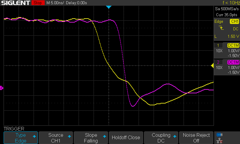
This screenshot was captured using a probe tip, ground spring setup which give a more accurate measurement than simply clipping the probes with longer lead/ground wires (which gave propagation delay of about 8 ns for the above measurement). I don’t have a comparable probe tip measurement for my third build but its propagation delay with just a simple measurement was about 18 ns. This is within spec for the 74HC11 used in that circuit.
I didn’t test whether the propagation delay varies for the more complex logic pathways. This is something I want to test in the future.
Going Forward
It’s likely my 4th build will not progress much beyond this point given my plans to continue on with the 65816. However, as I plan to use a PLD in that build, I hope that my 4th build will provide a useful test platform for various PLD logic ideas. And given that I wouldn’t want to do that with my third build, this build wasn’t a total waste of time. I’m getting a bit tired of cutting wires though.
PS
After testing that a basic 6502 build can run with a 65816 with a simple modification, I decided to modify build 4 to be more functional with both chips, including keyboard input and a bank address latch and data bus buffer needed for the 65816. I’ve been testing the build with both processors as I go along. The build with the data bus buffer works with both chips, though with some interesting challenges (a post on that is coming). However, I think a small modification will be needed to the bank address latch to run properly with the 6502.