I’ve mentioned previously having trouble getting WINCUPL to create the following memory map:
RAM  $0000-$7FFF
I/O  $8000-$80FF
ROM  $8100-$3FFFF
I figured that since I was expanding ROM, I might as well give myself a full 32k of RAM. WINCUPL didn’t like that though, giving me an error that it didn’t have enough pterms for my ROM_CS pin. I took the easy route and used the following map instead:
RAM  $0000-$7EFF
I/O  $7F00-$7FFF
ROM  $8000-$3FFFF
WINCUPL didn’t complain about that.
In expanding ROM, I simply connected pins A15-A17 to the address bus instead of to ground in my previous build. This means I’d waste the first 32k of the ROM of the address space, but no problem, I was gaining the rest of the space in the 256k ROM.
In considering how I’d add expanded RAM I figured I do the same with a 256k RAM chip (remember that my goal here is to build within the current footprint, so I couldn’t add separate expanded ROM and RAM chips). I’d be utilizing only half of the combined memory, but that’s still a win, being four times the memory of one of my 6502 builds.
Still, I wondered how WINCUPL would react to the non-consecutive RAM and/or ROM ranges that would be necessary. After all the 65xx processors require both RAM and ROM in the first 64k. I was also PLD constrained. I had used up all of my input and output pins.
I then recalled seeing others use an overlapping memory map, with something like:
RAM  $0000-$7EFF
I/O  $8000-$80FF
ROM  $8000-$FFFF
The I/O and ROM address ranges overlap. The ROM chip select logic code then excluded the I/O address range. Obviously WINCUPL didn’t object to that structure. I’d seen it successfully used.
I also recalled seeing the use of non-pin variables in WNCUPL code, with those variables used in the final output pin logic. If that worked, I should be able to combine address ranges into a single pin as well.
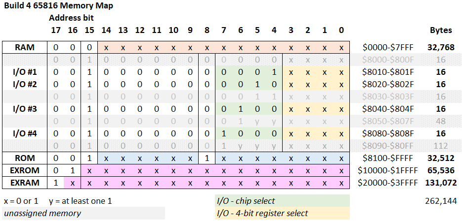
I tried out the following address map:
RAM   $0000-$7FFF
I/O   $8000-$80FF
ROM   $8000-$1FFFF
EXRAM $20000-$3FFFF
with the following logic:
!RAM_CS   = RAM # EXRAM;
!ROM_CS   = ROM & RW & !IO;
!IO_CS    = IO;
and it compiled just fine. Now to test it out.
Adding the Expanded RAM to Build 4
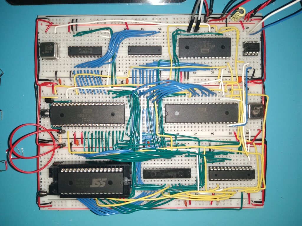
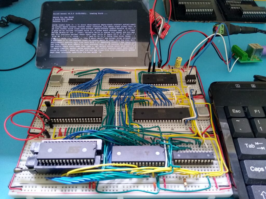
It’s just by chance that I have enough room to add a higher capacity RAM chip to my build. I’d left enough room around all of the build chips to allow for easy removal and replacement. The build was intended as a testbed after all. And while I hadn’t often had occasion to swap out RAM chips in my previous builds, in this one I had frequently had to swap between 55 ns and 12 ns RAM. My build had just enough space to squeeze in a new 32-pin, RAM chip.
As I was using a common address space to address my memory chips and didn’t have the luxury of adding additional chips or control signals, obviously I needed a RAM chip greater than 128k to reach the expanded RAM address space with my single RAM chip. Ideal would be a 256k chip that fit within the memory map above. The only size I found above this however was a 512k chip.
Luckily the common pins of the 32k and 512k chips had the same pinout except for the Vcc pin. This would be a simple addition.
One downside was that the 512k chip had an access time of 55 ns versus 12 ns for the 32k version. This build won’t be a particular speed demon. Though that really isn’t a goal for this breadboard build, I had hope to crank up the speed in my PCB version. I’d have to evaluate my options for that transition.
As an added benefit however, I could probably use the extra memory. If I used the PLD pin I reserved for a second VIA for address line A18 I’d gain access to the other 256k in the RAM. I’ll make that decision later though when I’m laying out my PCB for this project. I’ll probably have to get rid of either an extra VIA or ACIA anyway to make room for the bank address latch and data bus buffer chips. If I got rid of the VIA I’d gain an input pin on the PLD and then would have one free for address line A18.
Adding the chip was easy, but it was a tight fit as expected. I tested it out with the existing PLD after grounding address pins A15-18. The build started up and ran without problem.
Testing Expanded RAM
Wiring address pins A15-17 to the new 512k RAM chip was easy. They’re readily accessible on the PLD immediately to the right. I brought address line A18 down from the address bank latch in the upper left of the build. I probably could have just left this grounded. I don’t think the upper 256k is accessible without changes to my PLD setup. I’ll look into that later.
I fired up the system after updating the PLD with the logic discussed above and configuring my operating system for the new address map. My system started up successfully and I verified that some test code successfully could read from expanded ROM and write to and read from expanded RAM.
Great! I had just greatly expanded the memory of Build 4, about 96k ROM and 160k RAM. I still had a bit of work to do to access an additional 256k RAM.
PS
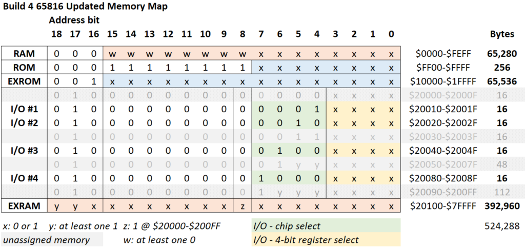
I’ll leave it to a PS to note getting access to the additional 256k of RAM. I verified, as I thought, that WINCUPL requires address line A18 to properly compile the larger expanded RAM address range. It was a simple matter to connect the A18 signal to the PLD in place of one that I had reserve for a second VIA interrupt request (tied high in the image above). Then the WINCUPL code and my operating system configuration were easily updated for the expanded RAM. Burning the ROM and PLD and starting up the system were successful. I verified I had access to the full ROM and RAM ranges. Here is the updated memory map.
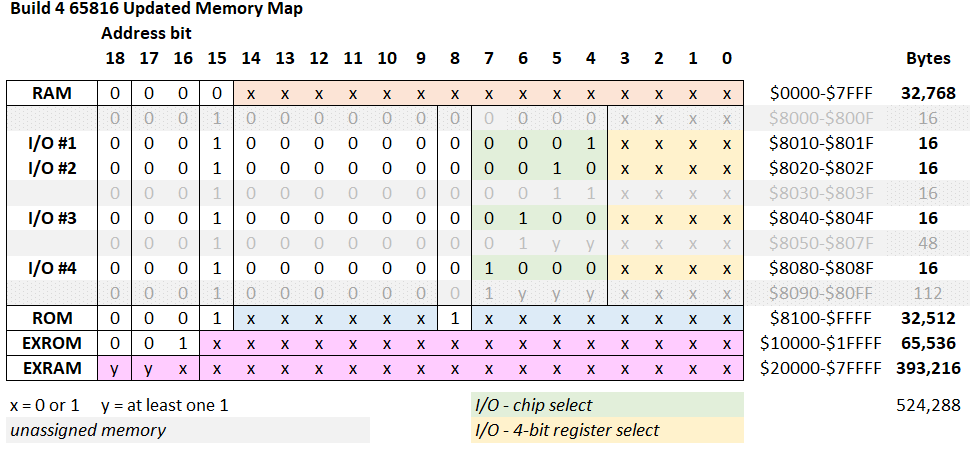
The build now has a total accessible memory of about 96k ROM and 416k RAM.
PPS
I’ve modified the memory map to take better advantage of Bank 0 memory for my Forth operating system. I plan to use Bank 0 RAM for direct page variables, the return stack and the Forth data stack. Bank 0 ROM is reserved for vectors and interrupt service routines. Bank 1 is reserved for read only code and data. The first page of Bank 2 is reserved for I/O. The remainder of memory is RAM.
The new memory map is:
RAM   $0000-$EFFF
ROM   $F000-$1FFFF
I/O   $20000-$200FF
EXRAM $20100-$7FFFF
I was able to accommodate this map in the ATF22V10 with the following logic:
RAM       = Address:[0000..FFFF];
ROM       = Address:[F000..1FFFF];
EXRAM     = Address:[20000..7FFFF];
IO        = Address:[20000..200FF];

!RAM_CS   = (RAM & !ROM) # (EXRAM & !IO);
!ROM_CS   = ROM & RW;
!IO_CS    = IO;
I tried to reduce Bank 0 ROM to a single page, which is all I currently need, but I couldn’t come up with logic that would fit within the PLD. I plan to do some more research on how others have accomplished single page regions, but given I already have a single page reserved for I/O, it’s quite possible I can’t get two.
The build now has a total accessible memory of 68k ROM and about 444k RAM.
PPPS – More research on PLD coding
As an example of the problems I was having coding my PLD, even the straight forward map representation below requires too many terms to fit within my PLD:
RAM       = Address:[0000..EFFF];
ROM       = Address:[F000..1FFFF];
IO        = Address:[20000..200FF];
EXRAM     = Address:[20100..7FFFF];

!RAM_CS   = RAM # EXRAM;
!ROM_CS   = ROM & RW;
!IO_CS    = IO;
It’s obviously easier to carve out small regions from larger ones. However, the very simple
RAM       = Address:[0000..7FFFF];
ROM       = Address:[F000..1FFFF];
IO        = Address:[20000..200FF];

!WE       = CLK & !RW;
!OE       = CLK & RW;
!RAM_CS   = RAM & !ROM & !IO;
!ROM_CS   = ROM & RW;
!IO_CS    = IO;
doesn’t work either as the contiguous RAM range is considered invalid. Trying
ROM       = Address:[F000..1FFFF];
IO        = Address:[20000..200FF];

!RAM_CS   = !ROM & !IO;
!ROM_CS   = ROM & RW;
!IO_CS    = IO;
doesn’t help as RAM_CS once again exceeds the capacity of the pin it’s assigned to (or any other for that matter). But then I wondered, why not base RAM_CS directly on ROM_CS and IO_CS, which have already been calculated. For example
ROM       = Address:[F000..1FFFF];
IO        = Address:[20000..200FF];

!ROM_CS   = ROM & RW;
!IO_CS    = IO;
!RAM_CS   = ROM_CS & IO_CS;
works! Then how about what I really wanted
ROM       = Address:[FF00..1FFFF];
IO        = Address:[20000..200FF];

!ROM_CS   = ROM & RW;
!IO_CS    = IO;
!RAM_CS   = ROM_CS & IO_CS;
This gave me insufficient terms on ROM_CS, but examining the pin details I saw that if I rearranged two pins, this would indeed fit within my PLD. Testing the new memory map in my build worked.
But was this definition of RAM_CS consistent with the more traditional address range approach? Looking at the RAM_CS, ROM_CS and IO_CS traces with my original memory map and PLD coding showed that one of the three was always selected.
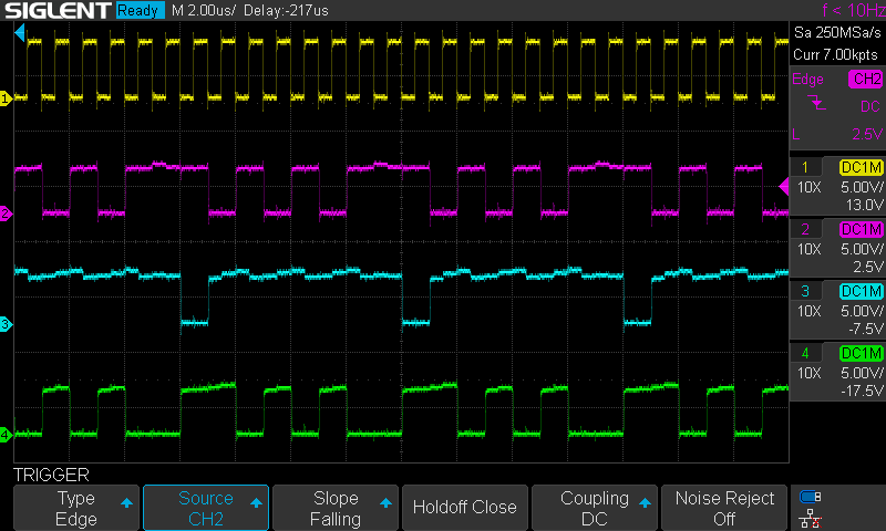
That made sense. The processor always had to be addressing some portion of memory.
Checking out the updated memory map and new PLD coding gave identical results.
I’ll continue to investigate for any times when this may not be valid, but for now at least, I’m calling this a success.
The build now has a total accessible memory of ~64k ROM and ~448k RAM. The new memory map is