I left Build 4 successfully running with the 65816 and 55 ns RAM. But it failed with memory corruption when I used 12 ns RAM.
The problem was that occasionally during RAM writes, some address signals would change about 2 ns before the write enable signal would rise.
This would result in a write to both addresses when the 12 ns RAM was installed. I discussed the problem in detail in this post.
The signals were the same with the 55 ns RAM but memory corruption didn’t occur. I assume this was because the 55 ns chip wasn’t able to react as fast to the changing address as the 12 ns chip. Thus its memory was not corrupted.
I also didn’t experience memory corruption with the 65C02 and 12 ns RAM. That combination worked becuase my 65C02’s actual address hold time is a bit longer than the minimum specification. With the 65C816, the actual hold time was exactly the specification, 10 ns.
I really wanted to get Build 4 running with the 12 ns RAM. My ultimate goal is to build a small handheld unit and the size of the 12 ns RAM chip was key to keeping the PCB to 100×100 mm, also a desired design goal. To make Build 4 run reliably with 12 ns RAM I needed to speed up the write enable signal by at least 2 ns.
Speeding Up the Write Enable Signal
One problem I had in speeding up the write enable signal was the PLD I was using for address decoding. It was fast, rated at 7 ns, but it wasn’t faster than the address decoder I used in my previous build. I didn’t have a faster alternative. The PLD also helped with some other design goals. While still a single chip address decoder, the same as Build 3, it provided a much more efficient memory map and eliminated a logic chip that Build 3 needed to combine interrupt request signals.
The rated propagation delay of the address decoder in my third build was comparable to that of the PLD but its actual delay was just 4 ns. The actual PLD propagation delay was more than double that.
This is when I remembered another difference between Build 3 and Build 4. In Build 3 (and the Ben Eater Build for that matter) the clock oscillator is next to the address decoder.
In Build 4 they’re on the opposite sides of the board.
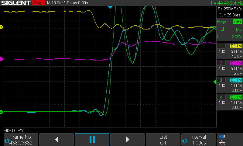
While I had previously examined all of the PLD output signals, I realized I had never looked at the PLD inputs. The result was telling. The PLD clock input signal (purple trace below) was delayed by 2 ns from the clock signal (yellow trace).
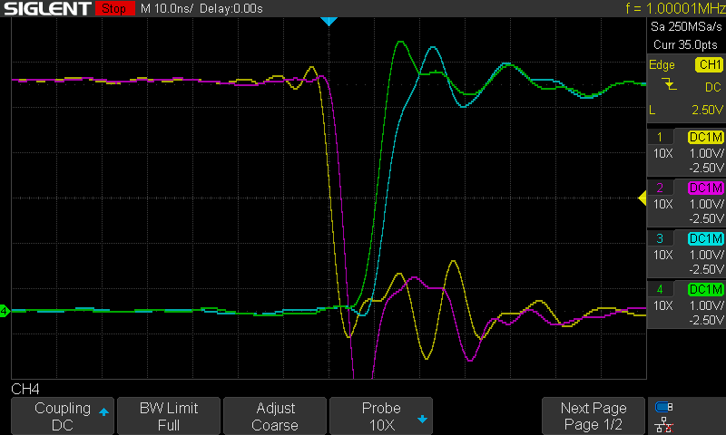
The delay was the result of about 8 inches of wire and several breadboard connections between the clock oscillator and the PLD (and everything in between, see PS at the end for a discussion). When I had laid out Build 4 originally, I had thought to keep the PLD close to the chips that would take control signals from it. I also wanted to keep the clock oscillator close to the processor. I didn’t particularly like the long wire run between the clock and the PLD, but I also didn’t think it would be the difference between success and failure.
I could gain most of the 2 ns back if I could get the clock oscillator closer to the PLD. A quick test with the clock oscillator on a separate board next to the PLD proved successful. Now, could I make the change on Build 4 itself. I didn’t want to add to the footprint or do any major rewiring.
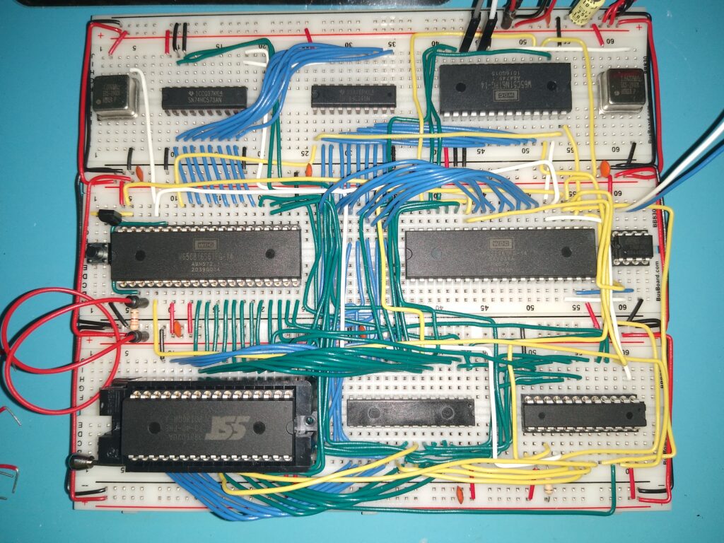
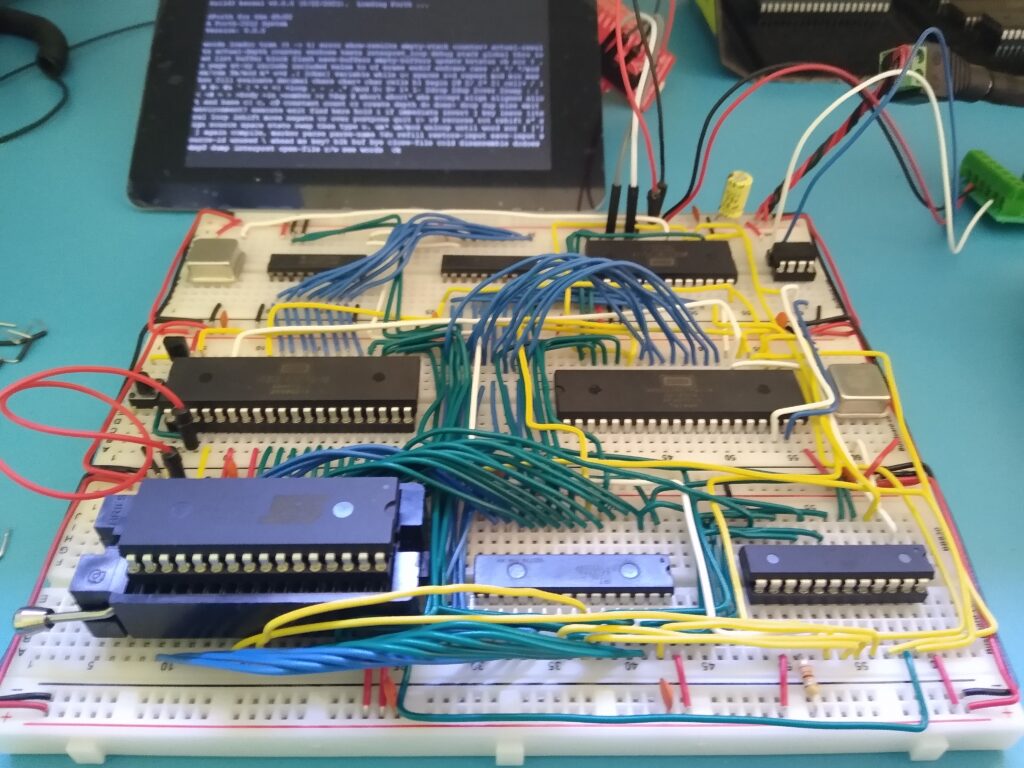
Examining the build I realized that fortuitously I had used half can clock oscillators and that the ATTiny85, which was exactly the same size, was located directly above the PLD. I could simply swap the two. That would require me to reroute the PS/2 keyboard signals back across the board to the VIA. A better alternaative was to also swap the ATTiny 85 with the ACIA clock oscillator, which was directly above it. That way the length of the PLD clock signal was greatly reduced and the length of some of the VIA and ACIA signals were slightly increased. These were less important as they were involved with I/O which occurs at much slower speeds.
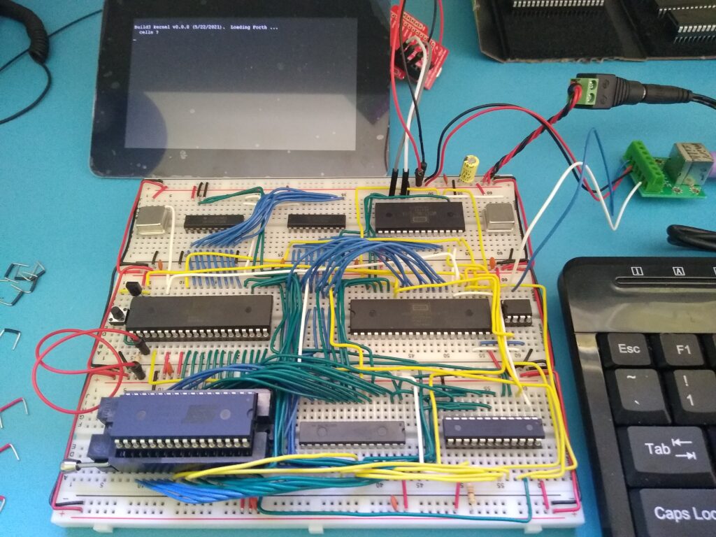
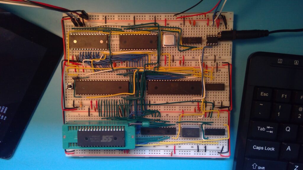
The final build didn’t even look that much different.
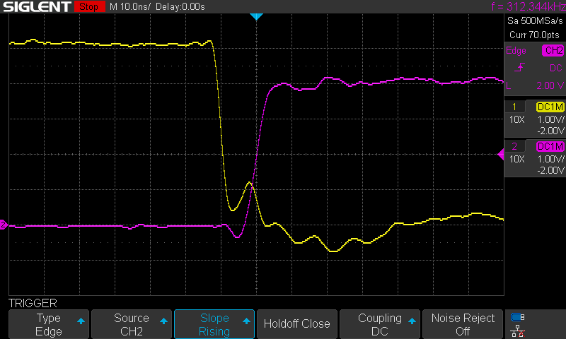
Checking out the RAM write enable signal compared to the address signal showed the expected result. The two rose in tandem, which was sufficient for my 12 ns RAM.
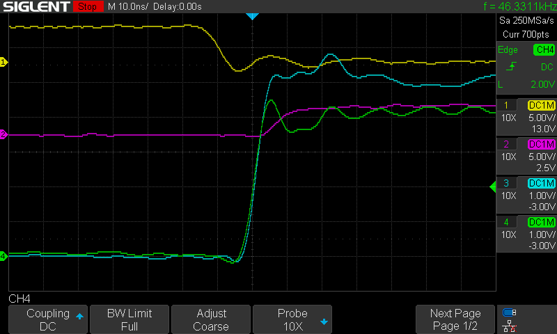
And the build started up and ran successfully.
This is all running with 74HC logic for both the bank address latch and data bus buffer. I’m not sure if I need any specific testing of the data bus buffer, given that it’s obviously working fine with my Forth operating system. But I’ll probably still do some probing to supplement my post on the W65C816SXB Development Board.
I also tried to access the banked memory beyond $FFFF in the expanded ROM without success. This isn’t surprising. My operating system is written for the 65C02 and has no way to set the 65816 processor’s bank address byte. I’ll be working on this next. I also just received some higher capacity SRAM chips. It just might be possible to cram one into the space occupied by the existing chip and it looks like only minimal rewiring is needed. More concerning is whether the PLD can accommodate an expanded RAM memory map. I have some thoughts to make it work. We’ll see how it goes.
PS
After I wrote this post, I still wondered at the 2 ns delay I saw between the clock and the PLD sitting at opposite sides of my breadboard build. A quick internet search (not verified) indicates that light travels about 1 foot in a nanosecond. For sake of argument, let’s assume our clock signal travels at the same speed. If so, I was seeing twice this delay in only 2/3 the distance. How much of this delay was caused by the distance and how much by the various breadboard connections between the two components, which were to facilitate wiring the clock to all of the chips that required the signal? Would a single wire of similar length have proved faster?
It wasn’t hard to create a mockup of my original clock signal layout on a breadboard, absent all of the chips of course. Accurate measurements of this are difficult with my oscilloscope, given its 200 MHz bandwidth but I was seeing something much closer to the theoretical than the delay I was seeing with the original layout. And there was no difference between the timing for the direct connection compared to the path with many breadboard transitions. As such, I assume the other chips in the original build, including the PLD itself, played a role in the 2 ns delay I was seeing.
It’s an open question whether a direct wire between the clock and the PLD would have been enough to solve my memory corruption problem. Based on my analysis here, I’m guessing not. It’s too much work to test out though, so for now it will remain an open question.
PPS
To be complete, I’ll note that I also tried a clock qualified chip select address decoding scheme with the PLD. The write to RAM in this scheme is controlled by the chip select signal rather than the write enable signal. The write enable signal is simply the processor’s read/write signal. For wiring I tried two options. The first just simply coded the PLD’s write enable output to be the same as the read/write input (that is the WE signal was delayed from the RW signal by the PLD’s propagation delay). I also tried wiring the RAM chip write enable pin directly to the processor. Neither of these tests solved my memory corruption problems. I didn’t pursue other PLD coding possibilities further, though I suppose there could be some additional things to explore there as well.