I worked on the Build 4 modifications over several weeks, partly because I was just playing around with what I had on hand when I started and partly getting sidetracked looking into why things happen instead of just getting on with the build. In this post I discuss one of those side investigations regarding the PLD that’s featured in this build. In another post, I discuss modifying Build 4 in more detail and in another post, I discuss troubleshooting the memory corruption issues I found.
While awaiting chips for my modifications to Build 4 I decided to get a jump start and test the 65816 data bus buffer circuit with chips I had on hand. I had LS and HCT versions of the 74xx245 chip needed for the buffer. I’ve discussed the modifications needed for this change in other posts, so I’ll just discuss my testing results and troubleshooting here.
I had no luck getting the build to run using the 74LS245 for the data bus buffer. Since I had the HCT version of the chip to test as well, I didn’t dive in to test why the chip wasn’t working for me. (Revisiting the chip on the completed modified Build 4 as I write this, the build runs the same as the other versions of the chip. I’m not sure why it wasn’t working before. As with other aspects of this build, it’s likely a combination of issues that I have since resolved, but at the time were either unknown or ambiguous.)
With the HCT245, I had the same startup issues that I’ve discussed in my other Build 4 posts. I won’t cover the specifics here again, but my system failed to start, giving an error code that reflected possible problems writing to RAM. Remember that this is early on in my testing and I naturally questioned whether my PLD was working correctly, and if it was in some way causing the issues I was seeing.
First, I worked up detailed timing diagrams for a data bus buffer assuming HC logic, the PLD’s typical propagation delay, and my 12 ns RAM. I may cover these in another post, but at the time I didn’t see anything that pointed to a problem with the design, either in reading from RAM or writing to it. I didn’t expect a theoretical timing problem moreover. WDC’s W65C816SXB Development Board works with similar timing and a 10 ns RAM after all. Of course, that isn’t a breadboard build, and my actual results could differ from the theoretical.
My suspicions towards the PLD being an issue were in part supported by what others were experiencing at the time. Reddit user wvenable was posting about problems he was having with his ATF22V10C PLD, the same one I was using. Wvenable was having trouble with the write enable signal from his PLD. This could explain my problem as well. Wvenable “solved” his problem by replacing the write enable signal with a separate logic circuit. That wasn’t the type of solution I was looking for though.
A bit later, Reddit user jowbi_wan posted that he solved a problem he was having with his 65816 build. Turns out he was using the same PLD. Could all of our problems be related to this PLD? I decided to break out my oscilloscope to check the signals coming from the PLD.
Examining the PLD Signals
The PLD takes input signals from the clock, processor and I/O devices and produces various system control signals. I discuss them in more detail in this post. Given that the build so far ran with the 65C02 but not with the 65816, I decided to compare the output signals from the PLD for each processor. It didn’t occur to me at the time to compare the input signals.
I took screenshots of all of the PLD output signals against the clock signal for both processors but I’m not going to review them here because they were basically the same. I’ll only highlight the ones for the I/O chip select signals where I noticed some spurious signals that I thought might be causing problems.
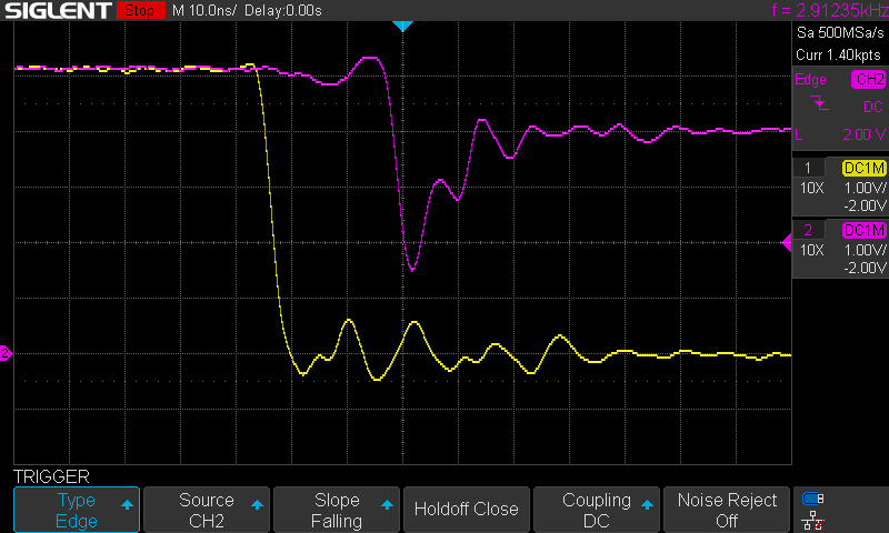


These were all captured during the startup portion of my code, but I couldn’t be certain they occurred doing the specific times I was having issues. I suspected I had memory corruption issues by this time and if these spurious signals occured at just the right time, I thought that the I/O device could be causing the problem. But I only had a 2-channel scope and needed more to fully investigate the issue. This isn’t the only time I’ve wished I had opted for a 4-channel scope, but the one I was considering when I got my oscilloscope was just too expensive to justify for a hobby.
I also wanted a 4-channel scope to look at the RAM timing. The clock, chip select, output enable and write enable signals are key there. I could look at two signals at a time, but a 4-channel scope would be handy.
I compared the RAM chip select signal versus the write enable signal for the 65C02 and didn’t see any issue. My code failed too quickly with the 65816 to get comparable captures. In any case, I wanted to include the clock and output enable signals as well.
About this time, I noticed that Siglent had released a more budget friendly version of their 4-channel scope. It had a lower bandwidth than my 2-channel scope but was still high enough that I thought it was a worthwhile troubleshooting tool. I placed an order. I discuss the screenshots I got from that scope in my memory corruption troubleshooting post.
While awaiting my new scope, I realized, after discussions with Reddit user wvenable, that I could use my logic analyzer to give me some information on what was happening with my build. My logic analyzer only portrays signals as high or low, but I realized that if I captured the signals at a high enough rate, I could glean some timing information as well.
I had previously only used my logic analyzer as a sort of monitor for my builds, decoding the address and data buses and examining the program flow to troubleshoot problems. This sometimes required me to use almost all of the analyzer’s 32 channels, somewhat limiting its bandwidth. But if I only needed to look at 8 or fewer signals, my logic analyzer had a bandwidth of 800 MHz. This is sufficient to somewhat reproduce the timing that I was seeing with my oscilloscope. Of course, you lost any detail of the transitions or the quality of the signal, but it was sufficient for telling whether a particular signal preceded some other signal by a certain amount of time.
Naturally I figured this all out after I had ordered the 4-channel scope. No matter, I’d discover that the signal details that the scope provides are important and ultimately, the problem I was having wouldn’t have been visible on the logic analyzer. In the meantime though, I used the logic analyzer to verify that the spurious I/O chip select signals were not occurring anywhere near RAM writes so it seemed that these weren’t the source of my problems.
The spurious signals do appear to be related to the PLD though. I don’t see similar signals from Build 3. And I still wonder if they could cause some issues at some point. But that’s an issue for another day.
PLD Programming Alternatives
Discussing these issues with wvenable on Reddit, I recalled reading a post over at 6502.org where the poster’s ATF22V10C wasn’t working correctly when programmed with the TL866 II+ programmer, the same one both wvenable and I were using. The problem was that the programmer provides two profiles for the PLD, one named ATF22V10C and the other ATF22V10C (UES). Apparently, the latter profile is needed to program a certain group of fuses in the PLD. I had been using the former profile, but decided to try the latter. As usual, I was a bit reluctant to do a lot of PLD testing given its limited number of programming cycles.
I reprogrammed the PLD with the ATF22V10C (UES) profile which seemed to solve my problem. Reddit user wvenable reported that it didn’t make a difference for his build. I didn’t do extensive testing so now I’m wondering if I was just experiencing one of those times that my build was actually working. I discovered later that the build would start up normally with the 65816 and 12 ns RAM if it had been shut down for some time. I still have additional PLD testing on my to do list. Their is a shortage of these chips right now so it could be some time before I’m able to continue with that investigation, not wanting to burn out the ones I have.
It’s the Memory, Stupid
I’d gone almost as far as I could at this point, given the troubleshooting tools that I had. Some common guidance recommends using parts with speed ratings appropriate for your build. I was using a 1 MHz clock and definitely didn’t need 12 ns RAM. I was using that chip however, for its narrow DIP package, giving me more freedom to wire multiple chips to the address and data buses, a usually tight fit on a breadboard. Unfortunately, I had used that extra space rather carelessly in my build and didn’t have room to drop in a slower RAM chip. So, I did the opposite. I increased the clock speed. It didn’t help.
My operating system is designed to operate at 1 MHz or above. I couldn’t run it at a slower clock speed. As such, the only way forward, at least until my new scope arrived, was to either write a different program for a slower clock or use a slower RAM chip. I relented and rewired the address and data bus lines to accommodate the wider DIP package of the slow RAM chips. I was reluctant to do this before because experience has proven that such changes can impact performance and operation. There was a good possibility that after these changes my results wouldn’t be comparable to those I’ve seen before.
Starting up the build with a 55 ns RAM chip proved successful. I thought I had solved my problem and told people so. After some testing however, I started noticing that my Forth data stack was getting corrupted. I didn’t do much testing because my new scope arrived about this time and I moved on to investigating the more immediate memory corruption with the 12 ns RAM. Is that corruption related to what I saw with the 55 ns RAM? They occur at much different points in the program so I can’t be sure. I tested the build again last night with the 55 ns RAM without problem, but I don’t think that settles the issue. More testing is needed.
So is the PLD Causing My Problems or Not
Looking at the ATF22CV10 PLD alone, I’m inclined to say that it’s doing exactly what I’ve programmed it to do (putting aside the spurious I/O chip select signals for a moment) and that it’s not involved with the 12 ns memory corruption I’m experiencing. It’s a fast PLD, with a rated 7 ns propagation delay. On many signals I’m seeing less than that. On a few, those with more complicated logic, I’m seeing somewhat more. These could be factors in the problems I’m having with the 12 ns RAM, but that is mainly driven by the issues I discuss in my next post on troubleshooting my memory corruption in detail. For now, I think the question on the PLD is an open issue. Others have used this PLD without issue. Given that my memory corruption appears to be related to the build and 65816 timing, I’ll assume the PLDs is working correctly for now. But it’s an open issue.